ULTIMATE –ELECTRONIC CAPTURE & PCB DESIGN
Copyright
Copyright c 1986 …1994 by Ultimate Technology. All rights reserved. No part of this manual may be reproduced by hard copy or any other copy method. Nor may it be translated into any other language without the prior written permission of Ultimate Technology.
Disclaimer
Although care was taken with respect to the contents of this document, ULTImate Technology reserves the right to make changes at any time without notice. No responsibility is assumed by ULTImate Technology for use of either the program or this information ; nor for any infringement of patents or other rights of third parties which may result from the use of this information of this product. Specifically, any implied warranties of merchantability or fitness for any particular purpose are disclaimed by ULTImate Technology.
Trademarks
ULTIcap , ULTIboard and ULTIroute GXR are registered trademarks of ULTImate Technology B.V.,Naarden NL.
ULTIMATE TECHNOLOGY
| International Headquarters ULTImate Technology B.V. Energiestraat 36 1411 AT Naarden The Netherlands Tel.: (+31) 2159-44444 , Fax.: (+31) 2159-43345 |
Belgium Sales Office ULTImate Technology Kardinaal Mercierplein 1 B-2800 Mechelen Tel.: (015) 401895 , Fax.: (015) 401897 |
| Support Centre USA/Canada Tel.: 1-800-267631 , Fax.: 519-6512259 |
U.K. / Ireland
Sales Office ULTImate Technology UK Ltd. 2 Bacchus House Calleva Park , Aldermaston Berkshire RG7, 4QW England Tel.: (0734) 812030 , Fax.: (0734) 815323 |
| Support Centre Germany Tel.: (030) 6959250 , Fax.: (030) 6942338 |
| How to use this manual | 5 |
||
| Software Installation | 7 |
Placing the traces | 20 |
| Hardware Setup - Starting the introduction | 7 |
Reroute while move | 22 |
| The User –interface | 7 |
Autorouting | 23 |
| Starting ULTIcap | 9 |
Requirements | 23 |
| From DOS | 9 |
Copper Area ’s | 24 |
| From Windows | 9 |
Let ’ s create the polygon | 24 |
| The Working area | 9 |
Creating Copper text | 26 |
| Placing the symbols | 10 |
Checking the design | 26 |
| Creating the netlist | 11 |
Connectivity errors | 27 |
| Manual wiring | 12 |
ULTIroute GXR | 27 |
| Autojunctions | 12 |
Requirements | 27 |
| Autowire | 13 |
Translating the board | 27 |
| Reroute while move | 14 |
For DOS users | 27 |
| Converting from ULTIcap to ULTIboard | 15 |
For Windows users | 28 |
| Conventions | 15 |
Costing | 28 |
| For DOS users | 15 |
Strategy | 28 |
| For Windows users | 16 |
Postprocessing | 30 |
| Starting ULTIboard | 17 |
For DOS users | 31 |
| Component placement | 17 |
For Windows users | 31 |
| Let’s finalize the board placement | 17 |
Using ULTIpost | 32 |
Following is a short description how this manual should be used. You should take action if the following line is shown ;
Please follow the commands as possible to maintain compatibility with this manual. Text printed with italic means that you should type something. Text between [LMB] means that a certain key or button should be pressed. Text in bold are menu selections.
All ULTlcap and ULTIboard systems come with an installation procedure that works for DOS or Windows. ALL ULTlcap & ULTIboard systems will run from MS-DOS or MS-Windows, the Windows installation creates an ULTImate group with all the appropriate icons and correct PIF settings.
Insert ‘disk 1 - Install’ in your floppy disk drive (A: or B:) and type A: INSTALL [enter]. The system will prompt you your serial number, user name and company name depending on the system you purchased (not for Demo disk & Evaluation Systems).
The installation program searches For Windows in your current search path and starts Windows (if you wish to abort the search for Windows press the spacebar).
The Installation prompts you to enter:
The disk space required will depend on the system and varies from approximately 6 - 12 Mb, the installation program checks whether the space for each system is available and creates an error message if you do not have enough.
You will also have to select o schematic capture package, and enter the directory name where the schematic system resides. The relevant interface files from and to your schematic package will be installed. If you are using ULTIcap the installation will suggest the default path, simply confirm the ULTImate directory with [enter]. The default ULTIcap library determines which library standard should be used, ANSI, IEC or both with a preferred search order.
Please insert the appropriate floppy disks as the system prompts you to. Make sure that you reboot the machine after the installation is completed. Remember to install the parallel dongle on either LPT1 , LPT2 or LPT3 depending on the system you purchased (not for Demo disk & Evaluation Systems).
Please refer to the supplied release notes for a detailed description of the installation of your system.
Hardware set-up :
The installation program copies all kinds of drivers into your ULTImate directory for your screen, your printer and your plotter output. The default set-up installs the standard VGA ‘screen driver, a HP LASER JET II printer driver, HP 7475 pen plotter driver and the GERBER 2000 photo plotter driver. These options can be changed later, but far the purpose of this introduction they are fine.
Starting the Introduction :
Once the software is copied to your hard disk, you are ready to start your ULTIcap & ULTIboard system. The way you should start and how you should use your ULTIcap & ULTIboard system depends if you wish to run from DOS or Windows
ULTISHELL V1.06
| Projects off Select workfile |
| Ulticap Schematics Ultiboard PCB |
| Annotate Schematic ULTIcap->ULTIboard Ultiboard->ULTIcap |
| Tools Postprocessing Libraries Configuration |
| Project managment |
| Quit |
ULTImate Technology NL 1988-1994
The User interface :
All the ULTlmate applications operate with the same user-interface, a pop-up menu structure that provides an uncluttered screen view during the editing modes. The left mouse activates a selection (or presents a new menu) and the right mouse button is used t o cancel the cornmand, or to go back to the previous selection.
There is no technical difference when running your ULTlcap & ULTIboard system from either DOS or Windows, there is just a minor difference in starting your applications.
From DOS :
Change to the default ULTlmate directory:
ULTIshell will bc presented, ULTIshell is a program that allows you to manage all your ULTImate applications to produce your complete design, from schematics to the final PCB artwork, all by mouse control!
-As mentioned earlier, a selection is made by moving your selection bar through the menus, and by activating the selected command with the Left Mouse Button (or [enter]). We will abbreviate Left Mouse Button to LMB, Middle Mouse Button to MMB and Right Mouse Button to RMB for the rest of this manual.
From Windows :
Windows multitasking capabilities allow you to launch an ULTIcap schematic, an ULTIboard PCB, your word processor etc. simultaneously. Once launched you can simply switch quickly between these applications by pressing ALT-TAB.
The Working area :
For the purpose of our introduction manual will load the Introduction schematic.
Probably the most important areas in schematic design are:
Placing the symbols :
If we look at retrieving and placing symbols first, ULTIcap offers you a number of powerful tools to do this easily , for example :
Unlike most of its competitors, ULTIcap does not use a separate Library Editor, we know it is much easier to create symbols as you design your schematic. All library symbols used in the schematic are stored with the schematic so you do not have to worry about Library management, your symbols are always available.
Let’s try some of these features, first retrieving by name :
As you can see there is no reference designator assigned yet, this is achieved later automatically with annotation tools.
Now let’s try to ‘copy’ a symbol from the screen:
Move the cross hair to the center of R3 (X:450,Y:2850) and click the LMB, you will see that the resistor is tied to the cross hair and you are ready to place the symbol, you are also able to rotate and mirror the symbol instantly:
Creating the netlist (placing the wires) :
ULTIcap offers you a number of powerful features to accurately draw your connections. As you know correct schematic capture is about more than just drawing a nice schematic for documentation, you are generating the netlist information upon which your PCB will be designed. It has got to be right!
You may have already experienced the all to common problems of missing junctions, wires overlapping pins or wires overlapping other wires. in other words what you see is definitely not what you get and more wasted PCBs end up in the bin.
ULTIcap avoids all these problems, firstly missed junctions are impossible as ULTIcap automatically places them as soon as you start or finish on a wire .Creating wire overlaps is also impossible because ULTIcap has a Snap to Pin function ensuring you are always connected correctly. Best of all though, if you move a wire ULTIcap’s Reroute While Move always maintains connectivity by stretching connections and avoids unwanted shorts by shoving other wires out of the way.
To speed up wiring you may decide to use ULTIcap’s Auto Wire feature, you click the pins, and ULTlcap draws the wires.
Manual wiring :
First we look at the manual wire mode :
As you can see it is impossible to create overlaps and unconnected pins with ULTlcap, this seems logical but there are many systems out there that do not have such a logical way of operation.
Autojunctions :
At each T-connection you create, ULTIcap automatically creates a junction dot to ensure the netlist is correct. With ULTIcap your design integrity is guaranteed:
Autowire :
To speed up your schematic capture, ULTIcap gives you Auto wire , an Autorouter for schematics! It allows you to simply click on the pins you wish to connect. Auto wire respects all your symbol boundaries and existing wires, and will never route through a symbol or overlap other connections.
Please complete the schematic as on the right:
Reroute While Move :
As you are creating an intelligent database while drawing the schematic
you are able to move the wires in such a way that connectivity remains, multiple wires can
be moved simultaneously with junctions. This move function is called Reroute While Move
since the auto wire is used to reroute your wires!
Let’s try it out:
After you have placed the symbols and wired them, you might have to move some of them. You are able with ULTIcap to move sections of the schematic while maintaining the connections with the block drag command. The block drag allows you to define an area within the schematic that should be ‘dragged’.
All connections are rewired without losing connections and maintaining all junctions with the On –line Electrical Rule Check. ULTIcap has been written with the emphasis on design integrity and we feel that ULTIcap provides an unrivaled array of features to help you meet this goal.
That was the introduction for ULTIcap Schematic package, we hope you understand that this was just a brief summary of the major features ULTIcap offers. For a more detailed explanation please consult the tutorial Manual . Please feel free to experiment with the other features and commands.
Converting from ULTIcap to ULTIboard :
Once the schematic is finalized, you are ready to generate a netlist and component list to be read into ULTIboard.
Conventions :
If you wish to interface your schematic from ULTIcap to ULTIboard the schematic must conform to the following conventions
When the symbols are placed from the libraries there are no reference designators (IC 1, R 1 etc.) attached to them, you can number them automatically with the Annotation tool found in ULTIshcll. The automatic annotation tool numbers all symbols on the schematic, even if gates are used over multiple sheets within a hierarchical structure.
Let's annotate the schematic and interface from ULTIcap to ULTIboard.
For DOS users :
At this moment the schematic is fully annotated, and you are ready to create the netlist and the component list:
For Windows users :
The annotation utility is started and will prompt you if you wish to display the report file on the screen, if you wish to print the report file (assuming to LPT1 :) or if you wish to abandon the report file and continue to process, press [D] to display the report file.
At this moment the schematic is fully annotated, and you are ready to create the netlist and the component list:
All the apropriate files are created and you are ready to read them from ULTIboard !
For DOS users :
Select ULTIboard PCB from the main menu of the ULTIshell [LMB]
For Windows users :
ULTIboard is started and loads the design INTRO.DDF as this is the current project. As you can see a similar screen as ULTIcap is shown, with the status bar on top of the screen and with some pop-up menu structure. ULTIboard starts with a default board outline, this is only a default size and may be changed at any time during the design cycle.
Component placement :
When the component list and the netlist are imported into ULTIboard, the components are placed initially outside the board outline, this design is partially placed for you. Since ULTIboard imports all pin to pin connections, the system is able to help you with a detailed placement and calculate the optimal placement for you. The REAL-TIME features to do this are:
Let’s finalize the board placement :
Now let’s see if the placement is done correctly :
As you can see ULTIboard tackles one of the most important areas of board design with powerful Real -Time Placement tools. The fact that these tools are also simple to use means that the time spent placing your designs will be significantly reduced.
Switch the Histograms off to continue wiring :
No matter what types of design you do thcrc will be a time when you need to manipulate the copper, manually adding traces, moving traces, adding copper-areas etc. Essential therefore to good design is the Real-time Design Rule Check that simply won’t allow shorts. Even better ULTIboard respects all the design rules given by you, the user! The Real-time Design Rule Check is operational during the placement of the traces, while moving the traces and while autorouting the board. So if the schematic is finalized and checked, a 100% correct PCB is guaranteed!
Placing the traces :
You have the ability to create designs with a maximum of 32 layers. ULTIboard will always assume that a 2 layer board is used (default), even if you wish to design a single sided board, simply use only one layer!
As you can see all pins connected to this pin light up and yellow service line is connected from this pin to the next nearest pin in the net, CTRL-F3 toggles to the next pin and back. At this moment You are connected to VCC, starting on the top layer and with trace code 3 (28 mil width and 13 mil clearance).The trace code (the width of the trace) is set either while drawing the schematic, or while importing the netlist, in this case the trace code for VCC & GND was set to 3 while drawing the schematic, the rest of the nets are set to code 1 (13mil width and 9 mil clearance) while importing the netlist. Trace code 1 is the default trace code.
If You move the cross hair a little bit away from the pad you would see that the trace connected to the pad is displayed as a dashed green line, indicating that you are connected to the pad and that you are starting a trace on the top layer (see also the status bar on top of the screen). If you click the middle mouse button the system will instantly change from top to the bottom layer.
Next you will introduce a via to change from the bottom layer back to the top layer, the middle mouse button changes from layer to layer while on a pad, if you are not connected to a pad a via will be introduced:
As you can see a via is introduced and the system continues at the top layer (see also the status bar).
Now let’s check out the Real-time Design Rule check:
Beep!!! And an error is detected, since this trace should not be connected to this pin as this pin belongs to an other net!
Again a beep that indicates a design rule error has occurred based upon the clearance from pad to trace! ULTIboard checks your actions in Real – Time and will not allow design rule errors.
The next feature we would like to show is the Reroute While Move feature, this is the command to move the copper traces while maintaining all the connections and checking in real time to ensure no errors are introduced.
Reroute While Move :
Let’s move some traces:
The trace is moved and with all connections maintained! Now move the trace a little bit further to see how the Real-time design rule check operates.
Beep!!! The system detects that a clearance error is created and does not allow the move!
Now let’s try to move a trace that contains vias:
Watch how the trace is moved with all its connections and vias, but also the trace that was in the way was shoved aside respecting all design rules over all 32 layers!!
The move Function is also capable of moving and stretching 45 degree corners in the copper.
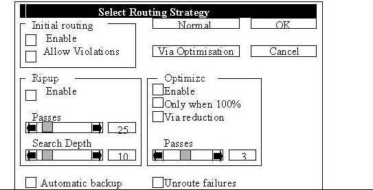
Autorouting :
All the ULTIboard packages include an internal autorouter, this is a gridless autorouter, that allows you to route per window, per component, per net and of course the complete board.
Requirements :
If you are planning to route a board with the help of the autorouter we suggest that you stick to the following rules:
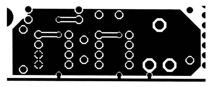
Let’s route the complete board:
The router starts to route the board, using the default settings . If the router achieves a 100% the via reduction will automatically start and will reduce the amount if vias. The routing process of this board will take approximately 1 minute on a 486 machine.
Copper Area’s (polygons) :
the polygon feature allows you to create copper areas on any layer, any shape. You simply draw the outline of the polygon and ULTIboard calculates all voids and connections that are required within the copper area. The connections that are created within the polygon are called thermal reliefs.
Let’s create a polygon 
The system starts with the calculation of the polygon with all the required voids and thermal reliefs. The calculation will take a couple of seconds.
Creating copper text :
ULTIboard allows you to place text on any of the copper layers and on the silk-screen.
Checking the design :
Although it is impossible to create clearance errors and shorts on the PCB we’ll always advise you to check the design once you are finished. Not just to check for shorts or clearance errors, but also for connectivity errors. To do so follow the next steps:
First we will check for clearance errors:
No errors are found! If an error was detected the system displays it on the screen with a white circle. Next we will check the design for connectivity errors.
The system starts to check the board and no errors are found.
You may have the Ripup & Retry auto router available in your ULTIcap & ULTIboard system depending on the system you purchased (not included with Challenger systems). ULTIroute GXR is a grid based auto router that runs from the Windows environment only. ULTIroute GXR is a stand alone external auto router which should be used to route the boards that are prepared within your ULTIboard system, the board should be placed and Power & Ground should preferably be routed before you translate the board to GXR.
Requirements :
Place the components within ULTIboard (we advise you not to use small placement grids).
Preroute the power & ground manually (if thicker traces arc used), or use powcrplanes for multilayer boards. Be aware that ULTIroute GXR is a grid based router which means that the router calculates the required grid for this board based upon the board size and the grid. The finer the grid, the slower the router gets, and the more memory you need.
Translating the board :
Since ULTIroute GXR is an external autorouter which reads a totally different database to ULTIboard, the board has to be translated before ULTIroute GXR can read it. We provided a board to test the router, it is a 4 layer board with powerplanes for VCC & GND on the inner layers. The GXR translator is not supplied with the Demo disk. Demo disk users may start ULTlroute GXR directly by double clicking the ULTIroute GXR icon from the program manager.
For DOS users :
ULTIroute GXR is not supported for the DOS environment! Please install Windows to be able to run ULTIroute GXR.
For Windows users :
The translator creates the router file and ULTIroute GXR is started with the converted PCB.
Costing :
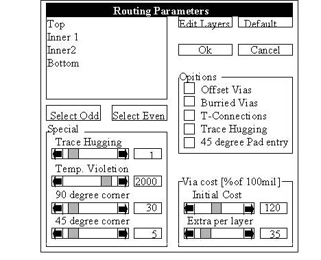
Since ULTIroute GXR is a cost based autorouter you have the ability to alter the costs that the router uses to route the board, let’s take a look at the costing dialogue window.
Strategy :
In this case the design is a 4 layer board with a powerplane for VCC & GND, let’s use the signal layers only to see if the router finalizes the board on two layers only:
The router starts to route the board and routes the board in approximately in 2 minutes on a 486 machine, now let’s enable the inner layers (the planes) to squeeze the last connections in:
Then we will finalize the board by starting the routing again:
The board is finalized in about 20 seconds on a 486 machine.
Next we will optimize the board to decrease the number of vias and to stretch the 45 degree corners.
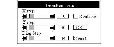
The optimization takes approximately 25 minutes on a 486 machine and does major cleanup as you can see! Remember the GXR is a cost based router, the costing of all settings may be different if the technology of you board varies from the board we used.
Costing that may effect routing dramatically are :
Once the board is routed and optimized you’ll only hove to translate it back to ULTIboard for Further manipulation:
At this moment the board is saved as a standard ULTIboard DDF file and can be read into ULTIboard for further manipulation, such as error checking, connectivity check and to create the output.
Postprocessing :
Final phase in the PCB design process is to create the output for PCB manufacturing.
You are able to create the following output data:
We use a separate utility to create all your output, called ULTIpost. The operation is very simple, you determine what you wish to print or plot per film ,(paper sheet), and with what kind of output device. The settings which determine what you would like to print or plot can be saved for future use. Let’s generate the output for a standard laser printer (HP LaserJet 300 DPI);
First we have to create a temporary file that is used by ULTIpost, start ULTIboard (if you already had quit ULTIboard, otherwise use ALT-TAB to switch to ULTIboard). First load the design INTRO.DDF
For DOS users :
For Windows users :
Using ULTIpost :
ULTIpost is started and you are ready to create your output, the status window on the right shows the default setup, which drivers will be used etc. ULTIpost assumes that there is no default setting file loaded, this setting file describes which item should be printed or plotted per film (paper sheet).
ART.PLS :
The settings are stored in a PLS. file , let’s load the standard PLS. for standard artwork for a double sided board:
ULTIpost starts to process the file, and creates an INTRO 1,L0, an INTRO 1 .L1, an INTRO 1 .L2 and an INTRO 1 .L3 file on the hard disk. You could also print the files directly to a hardware port, we advise you to output the files to hard disk so you can always print them again.
And the file is printed ! :
That’s it for this brief Introduction. We have only described a portion of the available features of ULTIcap and ULTIboard. If you would like more detailed information please refer to the Tutorial Manual. We have however pointed out the key features we feel put UCTIcap and ULTIboard above the competition in some of the most important areas of PCB design.
![]()
Right First Time Every Time !!